
The document introduces the CY2SSTU32864 data register, including its features such as operating frequency, supported DDRII SDRAM, two operating modes, operating voltage, and compatibility.
The CY2SSTU32864 is a 1.8 V data register that supports DDR‑II SDRAM with two operation modes: 25‑bit (1:1) and 14‑bit (1:2). It offers JEDEC‑compliant signaling, low‑power standby mode, and a 96‑ball FBGA package.
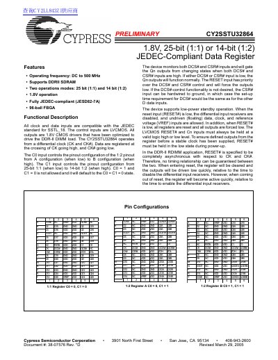
The document provides detailed pin configurations, absolute maximum ratings, electrical and timing specifications, test load setups, and ordering information for both commercial and tape‑and‑reel packaging.
| Operating frequency | DC to 500 MHz |
|---|---|
| Supply voltage (VDD) | 1.7 V – 1.9 V |
| JEDEC compliance | JESD82‑7A |
| Package type | 96‑pin FBGA (0° to 85°C) |
| Maximum operating temperature | 70 °C |
The device operates from DC up to 500 MHz.
It requires a VDD of 1.7 V to 1.9 V for normal operation.
Yes, it is fully JEDEC‑compliant according to JESD82‑7A.
It is supplied in a 96‑pin FBGA package suitable for commercial and tape‑and‑reel formats.