
AD9865 is a low-cost 3.3 V CMOS MxFETM for broadband modems. It features a 10-bit D/A converter, 2×/4× interpolation filter, 200 MSPS DAC update rate, integrated 23 dBm line driver with 19.5 dB gain control, 10-bit, 80 MSPS A/D converter, -12 dB to +48 dB low noise RxPGA(<3.0 nV/rtHz), third order programmable low-pass filter, flexible digital data path interface, half- and full-duplex operation, backward-compatible with AD9975 and AD9875, various power-down/reduction modes, internal clock multiplier (PLL), 2 auxiliary programmable clock outputs, available in 64-lead chip scale package or bare die.
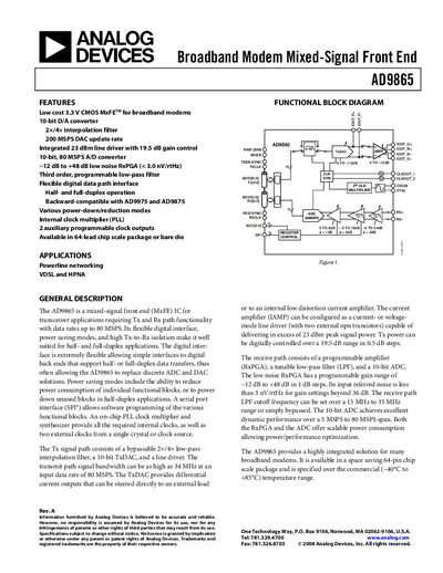
The AD9865 is a mixed‑signal front‑end (MxFE) IC designed for transceiver applications such as power‑line networking, VDSL and HPNA. It provides both transmit (Tx) and receive (Rx) paths with flexible digital interfaces, power‑saving modes, and high isolation for half‑ and full‑duplex operation. The Tx path includes a 10‑bit DAC, programmable interpolation filters and a line driver, while the Rx path features a programmable low‑noise PGA, tunable low‑pass filter and a 10‑bit ADC.
The device operates from a 3.3 V supply, includes an on‑chip PLL clock multiplier, and is available in a 64‑lead chip‑scale package. Detailed specifications cover resolution, update rates, gain ranges, power consumption, and timing for both half‑ and full‑duplex data interfaces.
| DAC Resolution | 10 bits |
|---|---|
| DAC Update Rate | 200 MSPS |
| Full‑Scale Output Current (IOUTP_FS) | 2.25 mA |
| AVDD Supply Voltage Range | 3.135 V – 3.465 V |
| Maximum Total Supply Current | 475 mA |
| Tx DAC Gain Range | -75 dB to 0 dB |
| RxPGA Gain Range | -12 dB to +48 dB |
| Power Consumption (Full‑Duplex, Analog) | 311 mA – 342 mA |
The AD9865 DAC provides a 10‑bit resolution.
The DAC can update at up to 200 MSPS.
It operates from a 3.3 V supply, with AVDD ranging from 3.135 V to 3.465 V.
The receive PGA gain can be programmed from –12 dB to +48 dB.