
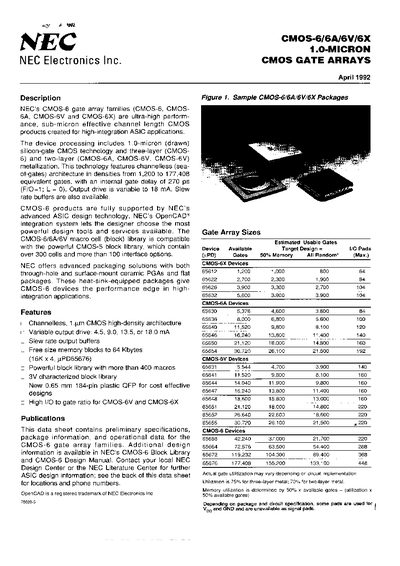
The NEC CMOS‑6 family of gate arrays uses a 1.0‑micron silicon‑gate CMOS process with channelless architecture, offering densities from 1,200 to 177,408 equivalent gates. The families provide variable output drive options (4.5 mA to 18 mA) and optional slew‑rate buffers for reduced noise and longer interconnects.
The datasheet includes absolute maximum ratings, DC characteristics, package options (including 0.65 mm QFP, PGA and PLCC), a full block‑library list, and contact information for NEC ASIC Design Centers worldwide.
| Process technology | 1.0‑micron silicon‑gate CMOS |
|---|---|
| Variable output drive | 4.5 mA, 9.0 mA, 13.5 mA, 18.0 mA |
| Internal gate delay (CMOS‑6) | 270 ps |
| Power‑supply voltage (VDD) | 0.5 V to 6.5 V |
| Operating temperature range | -40 °C to +85 °C |
| Maximum output current (18 mA drive) | 40 mA |
| Maximum usable gates (CMOS‑6X) | 177,408 |
The internal gate delay is specified as 270 ps.
Variable output drive options are 4.5 mA, 9.0 mA, 13.5 mA, and 18.0 mA.
The devices operate from –40 °C up to +85 °C.