
The MAX3228/MAX3229 are +2.5V to +5.5V powered EIA/TIA-232 and V.28/V.24 communications interfaces with low power requirements, and high data-rate capa- bilities, in a chip-scale package (UCSP™). The MAX3228/MAX3229 achieve a 1µA supply current with Maxim’s AutoShutdown™ feature. They save power without changes to existing BIOS or operating systems by entering low-power shutdown mode when the RS-232 cable is disconnected, or when the trans- mitters of the connected peripherals are off. The transceivers have a proprietary low-dropout trans- mitter output stage, delivering RS-232 compliant perfor- mance from a +3.1V to +5.5V supply, and RS-232 compatible performance with a supply voltage as low as +2.5V. The dual charge pump requires only four small 0.1µF capacitors for operation from a +3.0V sup- ply. Each device is guaranteed to run at data rates of 250kbps while maintaining RS-232 output levels. The MAX3228/MAX3229 offer a separate power-supply input for the logic interface, allowing configurable logic levels on the receiver outputs and transmitter inputs. Operating over a +1.65V to VCC range, VL provides the MAX3228/MAX3229 compatibility with multiple logic families. The MAX3229 contains one receiver and one transmit- ter. The MAX3228 contains two receivers and two transmitters. The MAX3228/MAX3229 are available in tiny chip-scale packaging and are specified across the extended industrial temperature range of -40°C to +85°C.
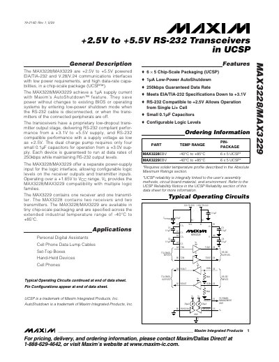
The MAX3228 and MAX3229 are low‑power RS‑232 transceivers that operate from +2.5 V to +5.5 V supply voltages. They feature Maxim’s AutoShutdown, reducing supply current to 1 µA when no valid RS‑232 signals are present, and they guarantee a 250 kbps data rate while maintaining RS‑232 output levels.
The devices are offered in a 6 × 5 UCSP (chip‑scale) package and support a separate logic‑level input (VL) from 1.65 V to 5.5 V, allowing configurable logic levels. Each part includes a dual‑mode regulated charge‑pump that generates ±5.5 V (or ±4.0 V at lower supply voltages) for the RS‑232 drivers, with hysteresis to prevent mode changes due to supply bounce. Pin configurations, absolute maximum ratings, and detailed electrical characteristics are provided for designers.
| Supply Voltage Range | +2.5 V to +5.5 V |
|---|---|
| Maximum Data Rate | 250 kbps |
| AutoShutdown Supply Current | 1 µA |
| Operating Temperature Range | -40 °C to +85 °C |
| Package | 6 × 5 UCSP |
The devices guarantee a data rate of up to 250 kbps.
The transceivers operate down to a supply voltage of +2.5 V.
In AutoShutdown the supply current is reduced to 1 µA.
Both parts are available in a 6 × 5 UCSP chip‑scale package.