
This document is a copyright statement from ICminer.com Electronic-Library Service. The service was created in 2003 to provide electronic library services. The document repeatedly contains the copyright statement.
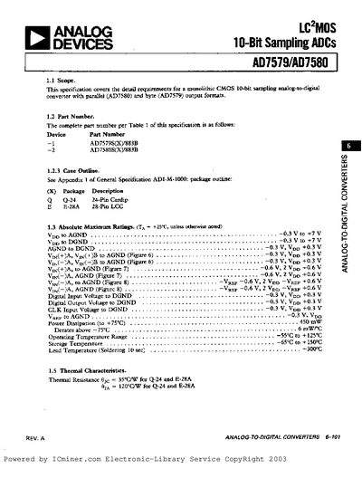
The AD7579 and AD7580 are monolithic CMOS 10‑bit sampling analog‑to‑digital converters offered in parallel (AD7580) and byte (AD7579) output formats. The document defines the scope, part numbers, package outlines, and absolute maximum ratings for the devices.
Key sections include functional block diagrams, timing specifications, thermal characteristics, life‑test burn‑in procedures, and application notes for both differential and single‑ended configurations. Electrical parameters such as input voltage ranges, clock limits, and power dissipation are provided for designers.
| Resolution | 10‑bit |
|---|---|
| Output format | Parallel (AD7580) and byte (AD7579) |
| Thermal resistance | 35 °C/W for Q‑24 and E‑28A |
| Input voltage range (Vpp to AGND) | –0.3 V to +7 V |
| Clock range | 250 kHz min to 25 MHz max |
| Signal‑to‑Noise Ratio (SNR) | ≥55 dB |
The AD7579 provides a byte‑parallel output, while the AD7580 provides a parallel output format.
The clock can operate from a minimum of 250 kHz up to a maximum of 25 MHz.