
AD7470/AD7472 is a 1.75 MSPS 10-bit/12-bit parallel ADC with features such as low power consumption, wide input bandwidth, and flexible power/throughput rate management.
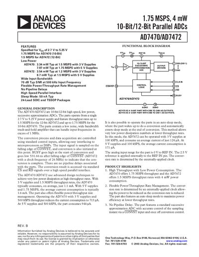
The AD7470 (10‑bit) and AD7472 (12‑bit) are high‑speed, low‑power successive‑approximation analog‑to‑digital converters that operate from a single 2.7 V to 5.25 V supply. They achieve up to 1.75 MSPS (AD7470) or 1.5 MSPS (AD7472) while consuming only a few milliwatts, and include an auto‑sleep mode for ultra‑low power at reduced throughput.
The document provides detailed pin‑out diagrams, timing specifications, absolute maximum ratings, and an ordering guide for various SOIC and TSSOP packages. It also describes the reference input requirements, power supply decoupling, and the logic functions of control pins such as CS, RD, CONVST, and BUSY.
| Resolution | 10 bits (AD7470), 12 bits (AD7472) |
|---|---|
| Throughput Rate | 1.75 MSPS (AD7470), 1.5 MSPS (AD7472) |
| Power Consumption (typical) | 3.34 mW at 1.5 MSPS, 3 V (AD7470); 8.7 mW at 1.5 MSPS, 5 V (AD7472) |
| Input Voltage Range | 0 V to REF IN (2.5 V) |
| Reference Input Voltage | 2.5 V ±1 % for specified performance |
The AD7470 can sample at up to 1.75 MSPS.
Typical power consumption is 8.7 mW under those conditions.
CS is the Chip Select input, active low, used with RD to access the conversion result.
A 2.5 V reference with ±1 % tolerance is required for specified performance.