
MAX9633 is a Maxim low-noise, low-distortion operational amplifier that is optimized to drive ADCs for use in applications from DC to a few MHz. The MAX9633 features low noise (3 nV/√Hz at 1 kHz and 3.5 nV/√Hz at 100 Hz) and low distortion (130 dB at 10 kHz), making it suitable for industrial, medical, and test applications. Its exceptionally fast settling time and low input offset voltage make it an excellent solution to drive high-resolution 12-bit to 18-bit SAR ADCs. The IC operates from a wide supply voltage range up to 36 V with only 3.5 mA of quiescent current per amplifier. The IC is offered in an 8-pin, 3 mm x 3 mm TDFN package for operation over the -40°C to +125°C temperature range.
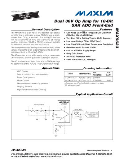
The MAX9633 dual operational amplifier offers very low input noise (3 nV/√Hz at 1 kHz) and low distortion (130 dB at 10 kHz), making it suitable for industrial, medical, and test applications that require high‑resolution ADC drivers. It operates from a wide supply range of 4.5 V to 36 V and consumes only 3.5 mA per amplifier.
Typical applications include ADC drivers for 12‑ to 18‑bit SAR converters, data acquisition, motor control, and high‑performance audio circuitry. The device is offered in 8‑pin TDFN and SOIC packages and is rated for operation from –40 °C to +125 °C.
| Low‑Noise | 3 nV/√Hz at 1 kHz |
|---|---|
| Low‑Distortion | 130 dB at 10 kHz |
| Settling Time | 750 ns to 16‑bit accuracy |
| Input Voltage Offset | 200 µV (max) |
| Gain‑Bandwidth Product | 27 MHz |
| Supply Voltage Range | 4.5 V to 36 V |
| Supply Current | 3.5 mA per amplifier |
| Package Types | 8‑Pin TDFN and SOIC |
The device operates from 4.5 V up to 36 V.
The MAX9633 settles to 16‑bit accuracy in about 750 ns.
Each amplifier draws approximately 3.5 mA of quiescent current.
The maximum input offset voltage is 200 µV.