
The MAX1932 is a low-noise, high-voltage output analog integrated circuit used to bias avalanche photodiodes (APDs) in optical receivers. The chip uses a constant-frequency, pulse-width modulated (PWM) boost topology combined with a unique architecture that maintains regulation with an optional RC or LC post filter inside its feedback loop, achieving very low output ripple and noise. The MAX1932 also integrates a precision reference voltage and error amplifier to maintain 0.5% output voltage accuracy. The MAX1932 protects expensive APDs against adverse operating conditions while providing optimal bias. Traditional boost converters measure switch current for protection, whereas the MAX1932 integrates accurate high-side current limiting to protect APDs under avalanche conditions. A current-limit flag allows easy calibration of the APD operating point by indicating the precise point of avalanche breakdown. The MAX1932 control scheme prevents output overshoot and undershoot to provide safe APD operation without data loss. The output voltage can be accurately set with either external resistors, an internal 8-bit DAC, an external DAC, or other voltage source. Output span and offset are independently settable with external resistors. This optimizes the utilization of DAC resolution for applications that may require limited output voltage range, such as 4.5V to 15V, 4.5V to 45V, 20V to 60V, or 40V to 90V.
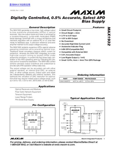
The MAX1932 generates a low‑noise, high‑voltage output to bias avalanche photodiodes (APDs) in optical receivers. It uses a constant‑frequency PWM boost topology with an internal 8‑bit SPI‑compatible DAC, providing 0.5 % output voltage accuracy and less than 1 mV ripple. The device includes high‑side current limiting and an avalanche indicator flag for safe APD operation.
Typical applications include optical receivers, fiber‑optic network equipment, telecom gear, laser range finders, and PIN‑diode bias supplies. The part is offered in a 12‑pin thin QFN package (4 mm × 4 mm) and can be configured via external resistors, an external DAC, or a voltage source.
| Input Supply Range | 2.7 V to 5.5 V |
|---|---|
| Output Voltage Range | 4.5 V to 90 V |
| Output Ripple | < 1 mV |
| Package | 12‑Pin Thin QFN, 4 mm × 4 mm |
| DAC Resolution | 8‑bit SPI‑compatible |
| Switching Frequency | 250 kHz to 340 kHz |
| Operating Temperature Range | -40 °C to +85 °C |
The device operates with an input supply between 2.7 V and 5.5 V.
Output voltage can be set with external resistors, the internal 8‑bit DAC, an external DAC, or another voltage source.
The CL pin goes low (CL = 0) when the device is in current‑limit mode; a logic high indicates normal operation.
The MAX1932 can deliver up to 90 V output.