
This document introduces the features and characteristics of ADP2503/ADP2504 600 mA/1000 mA, 2.5 MHz Buck-Boost DC-to-DC Converters.
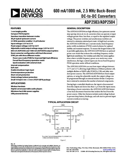
The ADP2503/ADP2504 are compact 10‑lead LFCSP buck‑boost converters that operate from 2.3 V to 5.5 V input and provide fixed or adjustable output voltages between 2.8 V and 5.5 V. Features include a 1 mm height profile, low quiescent current, internal compensation, soft‑start, and protection functions such as over‑temperature, short‑circuit, and undervoltage lockout.
Typical applications are wireless handsets, digital cameras, miniature hard‑disk power supplies, and USB‑powered devices. The datasheet includes pin descriptions, typical application circuits, performance graphs, PCB layout guidelines, and an ordering guide for the various fixed‑output and adjustable‑output part numbers.
| Input Voltage Range | 2.3 V – 5.5 V |
|---|---|
| Output Voltage Range | 2.8 V – 5.5 V |
| Switch Current Limit | 1.0 A (ADP2503) / 1.3 A – 2.0 A (ADP2504) |
| Oscillator Frequency | 2.1 MHz – 2.9 MHz |
| EN Input High Threshold | 1.2 V |
| Package Thermal Resistance | 84 °C/W (10‑Lead LFCSP) |
The devices operate from 2.3 V to 5.5 V input.
Fixed output versions are available from 2.8 V to 5.0 V, and an adjustable version can be programmed from 2.8 V to 5.5 V.
They are supplied in a 10‑lead LFCSP (QFN) package measuring 3 mm × 3 mm.