
This document describes the features and characteristics of the µPD4481161, µPD4481181, µPD4481321, and µPD4481361 ZEROSB static RAM chips. These chips are fabricated with advanced CMOS technology and feature high speed, low voltage, high density, and wide bit configuration. They are suitable for applications that require synchronous operation and buffer memory.
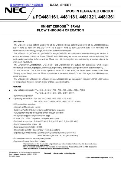
The NEC uPD4481161, uPD4481181, uPD4481321 and uPD4481361 are 8‑Mbit ZEROSB static RAMs fabricated with advanced CMOS technology. They provide synchronous flow‑through operation, burst read/write capabilities, and low‑voltage core supplies, making them suitable for high‑speed buffer memory applications.
These devices are offered in a 100‑pin plastic LQFP package and support both 3.3 V and 2.5 V LVTTL I/O levels. Power‑down mode is controlled by the ZZ pin, and various byte‑write enable pins (/BW1‑/BW4) allow selective data programming. Detailed pin configurations, timing specifications, and ordering information are provided in the sheet.
| Memory capacity (uPD4481161) | 524,288‑word by 16‑bit |
|---|---|
| Memory capacity (uPD4481181) | 524,288‑word by 18‑bit |
| Core supply voltage | Vop = 3.3 V + 0.165 V (or 2.5 V + 0.125 V) |
| Operating temperature range | 0 °C to 70 °C (‑40 °C to +85 °C for Y‑grade) |
| Package | 100‑pin plastic LQFP (14 × 20 mm) |
| Fast clock access time | 6.5 ns at 133 MHz |
The devices operate with a core supply of either 3.3 V (Vop = 3.3 V + 0.165 V) or 2.5 V (Vop = 2.5 V + 0.125 V) and are LVTTL compatible.
All four SRAMs are supplied in a 100‑pin plastic LQFP package measuring 14 × 20 mm.
Setting the ZZ pin HIGH puts the SRAM into the sleep (power‑down) state; setting it LOW returns normal operation.
Byte‑write enable is controlled by pins /BW1 through /BW4, with specific pins assigned per device variant.