
ADA4841-1/ADA4841-2 are low power, low noise and distortion, rail-to-rail output amplifiers.
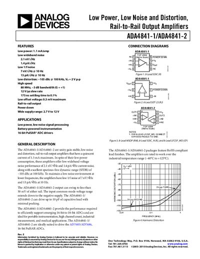
The ADA4841‑1 and ADA4841‑2 are unity‑gain stable, low‑noise, low‑distortion rail‑to‑rail output amplifiers. They consume only about 1.1 mA quiescent current while delivering a typical 80 MHz –3 dB bandwidth, 12 V/µs slew rate, and 175 ns settling time to 0.1 %.
These amplifiers are suited for battery‑powered instrumentation, 16‑bit PulSAR ADC drivers, and other high‑precision measurement applications. They are offered in 8‑lead SOIC, 6‑lead SOT‑23, 8‑lead MSOP, and 8‑lead LFCSP packages, with an operating supply range of 2.7 V to 12 V and a temperature range of –40 °C to +125 °C. The document includes connection diagrams, ordering guide, and typical performance graphs.
| Quiescent current | 1.1 mA |
|---|---|
| Input voltage noise (100 kHz) | 2.1 nV/√Hz |
| Operating supply range | 2.7 V to 12 V |
| Maximum supply voltage | 12.6 V |
| Capacitive load drive | 15 pF (30 % overshoot) |
The absolute maximum supply voltage is 12.6 V.
It can drive up to 15 pF with 30 % overshoot.
The device operates from –40 °C to +125 °C.