
The AD5381 is a 40-channel, 3V/5V, single-supply, 12-bit, voltage output DAC with the following features: guaranteed monotonic INL error: ±1 LSB max, on-chip 1.25V/2.5V, 10ppm/°C reference, temperature range: -40°C to +85°C, rail-to-rail output amplifier, power-down, package type: 100-lead LQFP (14mm x 14mm), user interfaces: parallel serial (SPI®-/QSPI™-/MICROWIRE™-/DSP-compatible, featuring data readback) I2C®-compatible
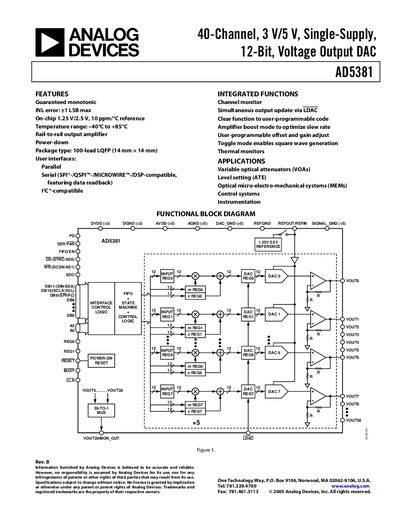
The AD5381 is a single‑supply, 40‑channel, 12‑bit DAC offered in a 100‑lead LQFP package. Each channel includes an on‑chip output amplifier with rail‑to‑rail operation, a programmable internal 1.25 V/2.5 V reference, and a channel‑monitor function that multiplexes the analog outputs to a common MON_OUT pin for external monitoring. The device also features an output‑amplifier boost mode to optimize slew rate.
The DAC provides a double‑buffered parallel interface with a 20 ns WR pulse width and a serial interface compatible with SPI, QSPI, MICROWIRE and DSP protocols, supporting speeds over 30 MHz. Both AD5381‑5 (AVDD 4.5‑5.5 V) and AD5381‑3 (AVDD 2.7‑3.6 V) variants are available, operating over a temperature range of –40 °C to +85 °C.
| Resolution | 12 Bits |
|---|---|
| Number of Channels | 40 |
| AVDD Supply Voltage (AD5381‑5) | 4.5 V to 5.5 V |
| AVDD Supply Voltage (AD5381‑3) | 2.7 V to 3.6 V |
| Output Voltage Range | 0 V to AVDD |
| Short‑Circuit Current | 40 mA max |
| Load Current | 1 mA max |
| Power Consumption (unloaded, boost off) | 0.375 mA per channel max |
| Operating Temperature Range | -40 °C to +85 °C |
| INL (Integral Nonlinearity) | +1 LSB max |
| DNL (Differential Nonlinearity) | +1 LSB max |
| Gain Error | +0.024 % FSR max |
| Power Dissipation (AD5381‑5) | 80 mW max |
The AD5381‑5 operates with AVDD from 4.5 V to 5.5 V and DVDD from 2.7 V to 5.5 V.
The AD5381 provides 40 independent output channels.
The device can source up to 40 mA in a short‑circuit condition and supports a continuous load current of up to 1 mA per channel.