
This data sheet introduces the features of Analog Devices's ADA4898-1/ADA4898-2 high voltage, low noise, low distortion, unity-gain stable, high speed operational amplifier
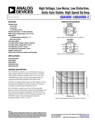
This document describes the ADA4898‑1 and ADA4898‑2 ultra‑low‑noise, low‑distortion, unity‑gain stable voltage‑feedback op‑amps. It covers features, typical applications such as instrumentation, active filters, DAC buffers, SAR ADC drivers, and optoelectronics, and provides a general description of the device architecture and package.
Detailed specifications are given for dynamic performance (bandwidth, slew rate, settling time), noise and distortion, DC characteristics, input and output parameters, power‑supply requirements, absolute maximum ratings, thermal resistance, and pin functions. The handbook also includes connection diagrams, typical performance graphs, and revision history.
| Supply Voltage Range | +5 V to +16 V |
|---|---|
| –3 dB Bandwidth (typ) | 65 MHz |
| Input Voltage Noise (1 kHz) | 0.9 nV/√Hz |
| Input Current Noise (1 kHz) | 24 pA/√Hz |
| Supply Current (per amp) | 8 mA |
| Input Offset Voltage (max) | 160 pV |
| Absolute Maximum Supply Voltage | 36 V |
The ADA4898‑1 and ADA4898‑2 operate from +5 V up to +16 V.
The input voltage noise is 0.9 nV/√Hz at 1 kHz.
The –3 dB bandwidth is 65 MHz.
The PD pin powers down the device when a voltage below –14 V is applied; a voltage between 2 V and 13 V enables the chip.