
The ADA4001-2 is a dual channel JFET amplifier that features low input voltage noise and current noise, input bias current, and rail-to-rail output. The combination of low noise and low input bias current makes this amplifier ideal for a variety of measurement applications, including instrumentation, medical instruments, multipole filters, precision current measurement, photodiode amplifiers, and audio amplifiers.
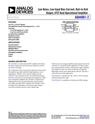
The ADA4001-2 dual JFET amplifier offers very low input voltage noise (1.2 µV rms, 20 Hz‑20 kHz) and low input bias current (20 pA typical) while providing rail‑to‑rail output and unity‑gain stability. Its fast settling performance and high output current make it suitable for medical instruments, precision current measurement, photodiode amplifiers, audio, and sensor applications.
The device is supplied in an 8‑lead narrow SOIC (R‑8) package and operates over a wide temperature range (‑40 °C to +125 °C) with a supply voltage range of +5 V to +18 V. Key electrical characteristics include a slew rate of about 25 V/µs, gain‑bandwidth product of 16.7 MHz, and a power‑supply rejection ratio of 96‑110 dB.
| Input Bias Current | 20 pA typical |
|---|---|
| Voltage Noise (20 Hz‑20 kHz) | 1.2 µV rms |
| Slew Rate | ≈25 V/µs |
| Gain‑Bandwidth Product | 16.7 MHz |
| Power‑Supply Rejection Ratio | 96‑110 dB |
| Operating Voltage Range | +5 V to +18 V |
| Package | 8‑lead narrow SOIC (R‑8) |
| Temperature Range | ‑40 °C to +125 °C |
The typical input bias current is 20 pA at a supply voltage of +15 V.
It operates from –40 °C up to +125 °C.
It is supplied in an 8‑lead narrow SOIC (R‑8) package.
The absolute maximum supply voltage is +18 V.