
AD5763 is a 16-bit high precision dual channel analog digital converter produced by Analog Devices (ADI). The product can be programmed to output in the range of ±4.096V, ±4.201V or ±4.311V, with a maximum INL error of ±1LSB and a maximum DNL error of ±1LSB. The product has low noise, 10μs maximum settling time, integrated reference buffers, on-chip temperature sensor, power-up/brownout output control, programmable short-circuit protection, simultaneous updating via LDAC, asynchronous clear to zero code, digital offset and gain adjustment, logic output control pins, and DSP/microcontroller compatible serial interface. The product's temperature range is -40℃ to +105℃, and it uses iCMOS® technology.
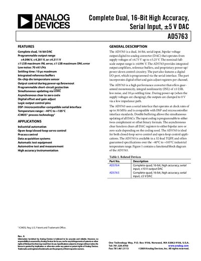
The AD5763 is a dual, 16‑bit, serial‑input, bipolar voltage‑output DAC that operates from a supply of 4.75 V to 5.25 V. It offers programmable output ranges (+4.311 V, +4.201 V, +4.096 V), low noise (70 nV/√Hz), and integrated reference buffers, making it suitable for industrial automation, test equipment, and high‑accuracy instrumentation.
The datasheet provides detailed specifications such as resolution, INL/DNL, output voltage ranges, timing characteristics, and absolute maximum ratings. It also includes functional block diagrams, pin descriptions, layout guidelines, and ordering information for the 32‑lead TQFP package.
| Resolution | 16 Bits |
|---|---|
| Integral Nonlinearity (INL) | ±1 LSB |
| Differential Nonlinearity (DNL) | ±1 LSB |
| Supply Voltage Range | 4.75 V to 5.25 V |
| Operating Temperature Range | –40 °C to +105 °C |
| Output Voltage Range (Coarse Gain 0) | ±4.096 V |
| Settling Time (Full‑scale step) | 10 µs max |
The AD5763 operates from a supply voltage of 4.75 V to 5.25 V.
The device is specified for operation from –40 °C to +105 °C.
The AD5763 provides a 16‑bit resolution.
The typical settling time is up to 10 µs for a full‑scale step.