
The AD7804/AD7808 are quad/octal 10-bit digital-to-analog converters, with serial load capabilities, while the AD7805/AD7809 are quad/octal 10-bit digital-to-analog converters with parallel load capabilities. These parts operate from a +3.3 V to +5 V (±10%) power supply and incorporates an on-chip reference. These DACs provide output signals in the form of VBIAS ± VSWING. VSWING is derived internally from VBIAS. On-chip control registers include a system control register and channel control registers. The system control register has control over all DACs in the package. The channel control registers allow individual control of DACs. The complete transfer function of each individual DAC can be shifted around the VBIAS point using an on-chip Sub DAC. All DACs contain double buffered data inputs, which allow all analog outputs to be simultaneously updated using the asynchronous LDAC input.
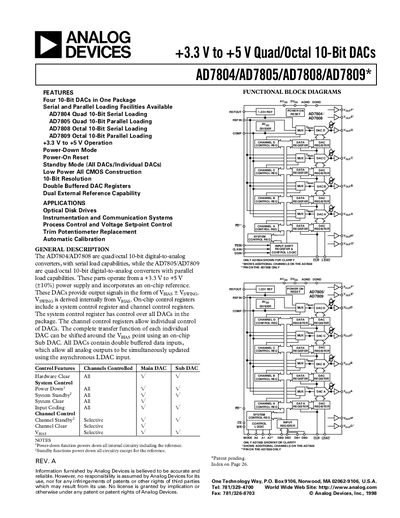
The AD7804, AD7805, AD7808, and AD7809 are quad or octal 10‑bit digital‑to‑analog converters that operate from a +3.3 V to +5 V supply. They offer serial or parallel loading, on‑chip reference, dual external reference capability, and low‑power modes such as standby and power‑down.
The document includes detailed electrical specifications, timing characteristics for both serial and parallel loading, absolute maximum ratings, pin‑function tables, mechanical outline dimensions, and an ordering guide for the various package options.
| Resolution | 10 bits |
|---|---|
| Relative Accuracy | +3 LSB max |
| Gain Error | +3 % FSR max |
| Supply Voltage Range | 3.3 V to 5 V |
| Power‑Down Current (25 °C) | 0.8 µA max |
| Power Dissipation (Normal Mode) | 66 mW max |
The reference output (REF OUT) is nominally 1.23 V.
The devices are rated for operation from –40 °C to +85 °C.
The main DACs provide 10‑bit resolution.
The power‑down current is 0.8 µA maximum at 25 °C.