
The MAX6625/MAX6626 combine a temperature sensor, a programmable overtemperature alarm, and an I2C- compatible serial interface into single compact packages. They convert their die temperatures into digital values using internal analog-to-digital converters (ADCs). The result of the conversion is held in a temperature register, readable at any time through the serial interface. A dedi- cated alarm output, OT, activates if the conversion result exceeds the value programmed in the high-temperature register. A programmable fault queue sets the number of faults that must occur before the alarm activates, prevent- ing spurious alarms in noisy environments. OT has pro- grammable output polarity and operating modes. The MAX6625/MAX6626 feature a shutdown mode that saves power by turning off everything but the power-on reset and the I2C-compatible interface. Four separate addresses can be configured with the ADD pin, allowing up to four MAX6625/MAX6626 devices to be placed on the same bus. The MAX6625P/MAX6626P OT outputs are open drain, and the MAX6625R/MAX6626R OT outputs include internal pullup resistors. The MAX6625 has a 9-bit internal ADC and can function as a replacement for the LM75 in most applications. The MAX6626 has a 12-bit internal ADC. Both devices come in the space-saving 6-pin SOT23 package, or the 6-pin TDFN package.
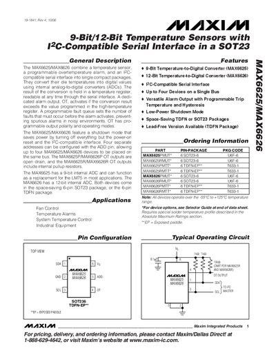
The MAX6625/MAX6626 combine a temperature sensor, a programmable over‑temperature alarm, and an I2C‑compatible serial interface in compact 6‑pin SOT23 or TDFN packages. They continuously convert die temperature to digital values using on‑chip delta‑sigma ADCs and provide the result via a temperature register readable at any time.
Both devices support up to four unique I2C addresses, a shutdown mode that reduces power consumption, and configurable alarm polarity. The MAX6625 offers a 9‑bit ADC (0.5 °C resolution) while the MAX6626 provides a 12‑bit ADC (0.0625 °C resolution). Operating temperature range is –55 °C to +125 °C, with a supply voltage of 3.0 V to 5.5 V.
| ADC Resolution | 9‑bit (MAX6625) / 12‑bit (MAX6626) |
|---|---|
| Supply Voltage Range | 3.0 V to 5.5 V |
| Operating Temperature Range | -55 °C to +125 °C |
| I2C Bus Device Count | Up to four devices on a single bus |
| OT Output Type | Open‑drain (P‑type) or internal pull‑up (R‑type) |
The devices operate with a supply voltage from 3.0 V to 5.5 V.
Up to four devices can be placed on a single I2C bus by configuring the ADD pin.
Each conversion cycle takes about 130 ms.
The MAX6626 provides a temperature resolution of 0.0625 °C per LSB.