
The TC4431/TC4432 are 30V CMOS buffer/drivers suitable for use in high-side driver applications.
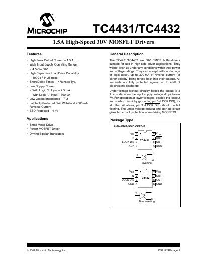
The TC4431 and TC4432 are 30 V CMOS buffer/drivers designed for high‑side MOSFET driver applications. They feature a wide supply range, high peak output current, and built‑in latch‑up and ESD protection. The devices can tolerate up to 300 mA of reverse current and include an under‑voltage lockout circuit that can be disabled via the LOCK DIS pin.
Key specifications include a 1.5 A peak output current, 4.5 V‑30 V supply range, low output impedance, and fast switching times (rise < 40 ns, fall < 50 ns). Pin descriptions, typical performance curves, and packaging details are provided to aid designers in implementing the drivers in motor‑drive, power MOSFET, and transistor‑driving circuits.
| Peak Output Current | 1.5 A |
|---|---|
| Supply Voltage Range | 4.5 V to 30 V |
| Logic ‘1’ Input Voltage (Vih) | 2.4 V |
| Logic ‘0’ Input Voltage (Vil) | 0.8 V |
| Output Resistance | 7 Ω |
| Rise Time | 25‑40 ns |
| Fall Time | 33‑50 ns |
| Delay Time (typ.) | 78‑90 ns |
| Latch‑Up Protection Reverse Current | >300 mA |
The devices can source up to 1.5 A of peak output current.
They operate with a supply voltage between 4.5 V and 30 V.
Tie pin 3 (LOCK DIS) to ground to disable the lockout circuit.
Typical rise time is 25‑40 ns, fall time 33‑50 ns, and delay time about 78‑90 ns.