
The TC7660 is an integrated circuit that uses two external capacitors to convert a +1.5V to +10V input to a corresponding -1.5V to -10V output, replacing the industry standard 7660 charge pump voltage converter.
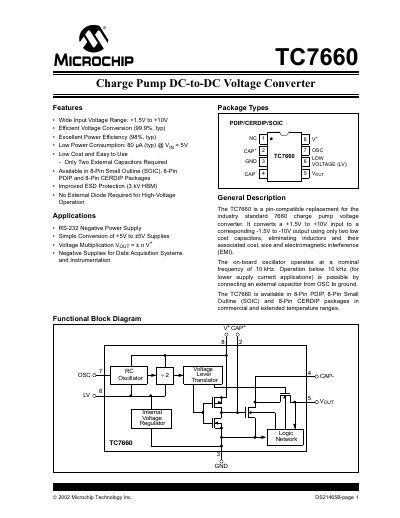
The TC7660 is a charge‑pump DC‑DC voltage converter that inverts a +1.5 V to +10 V input into a corresponding –1.5 V to –10 V output using only two external capacitors. It offers a wide input range, high conversion efficiency, and low power consumption, making it suitable for RS‑232 negative supplies, simple +5 V to –5 V conversion, and data‑acquisition systems.
The document includes electrical characteristics, typical performance curves, pin functions, and application notes such as simple negative conversion, device paralleling, cascading, and oscillator frequency adjustment. Package options include 8‑pin PDIP, SOIC, and CERDIP, and the device is available in commercial and extended temperature ranges.
| Input Voltage Range | +1.5 V to +10 V |
|---|---|
| Voltage Conversion Efficiency | 99.9 % typ |
| Supply Current | 80 µA typ @ Vin=5 V |
| Power Efficiency | 95 % – 98 % typ |
| Output Source Resistance (Rout) | 70 Ω – 100 Ω |
| Oscillator Frequency | 10 kHz |
The device operates from +1.5 V up to +10 V input.
Only two external capacitors are needed for the charge‑pump operation.
Pin 2 (CAP*) is the positive capacitor terminal and pin 4 (CAP') is the negative capacitor terminal.