
The LTC4253/LTC4253A negative voltage Hot Swap controllers allow a board to be safely inserted and removed from a live backplane. Output current is controlled by three stages of current-limiting: a timed circuit breaker, active current limiting and a fast feedforward path that limits peak current under worst-case catastrophic fault conditions.
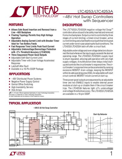
The LTC4253 and LTC4253A are negative‑voltage hot‑swap controllers with sequencer that enable safe board insertion and removal from a live -48 V backplane. They provide adjustable analog current limiting, fast fault current limiting, undervoltage/overvoltage protection, and three sequenced power‑good outputs.
This manual describes the device features, absolute maximum ratings, package information, detailed electrical specifications, typical performance curves, pin functions, application information, related parts, and recommended PCB layout guidelines.
| Maximum Junction Temperature | 125 °C |
|---|---|
| Input Voltage Range (except SENSE/DRAIN) | -0.3 V to 16 V |
EN2 is a TTL‑compatible input that controls the PWRGD2 and PWRGD3 power‑good outputs; driving it low forces both outputs high, while driving it high allows sequencing of the power‑good signals.
The SS pin ramps the inrush current during start‑up; an internal current source charges the SS capacitor, and the pin voltage limits the MOSFET drain current to control the soft‑start current.
The device is rated for a maximum junction temperature of 125 °C.
The input voltage (except for SENSE and DRAIN pins) may range from –0.3 V to 16 V.