
This document describes the features and characteristics of the high-performance power combi controller TDA 16888, including the functions and operating modes of the PFC section and PWM section.
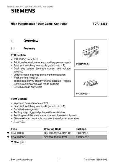
The TDA 16888 is a high‑performance power combi controller that integrates PFC and PWM sections with dual‑loop control, auxiliary power supply capability, and a wide input voltage range. It supports both boost/flyback (PFC) and forward/flyback (PWM) topologies and offers soft‑switching gate drives.
The document provides pin definitions, functional blocks such as over‑voltage and under‑voltage protection, oscillator synchronization, and package outlines for the P‑DIP‑20‑5 and P‑DSO‑20‑1 variants. Protection features include internal Zener diodes, fast over‑voltage circuitry, and ESD protection on all pins.
| Input voltage range | 90 V to 270 V |
|---|---|
| Maximum PFC duty cycle | 94 % |
| Maximum PWM duty cycle | 50 % |
| Stand‑by supply current (start‑up) | Typical 50 pA |
| Quiescent current | 15 mA |
| Over‑voltage protection threshold | Above 17.5 V |
| Undervoltage lockout thresholds | Stand‑by at ≤14 V, shutdown at ≤11 V |
The device operates with input voltages ranging from 90 V to 270 V.
It uses an internal Zener diode at pin 9 and a fast over‑voltage protection circuit at pin 19 to shut down the gate drives when the voltage exceeds the limit.
The PFC section can operate with a maximum duty cycle of about 94 %.
By applying an external clock to pin 12 (SYNC) and adjusting the external resistor at pin 16 (ROSC) to set the desired frequency range.