
AD7870/AD7875/AD7876 is a monolithic 12-bit ADC from Analog Devices. It consists of a 2µs track/hold amplifier, an 8µs successive-approximation ADC, a 3V buried Zener reference and versatile interface logic. The ADC features a self-contained internal clock which is laser trimmed to guarantee accurate control of conversion time. No external clock timing components are required; the on-chip clock may be overridden by an external clock if required. The device offers a choice of three data output formats: a single, parallel, 12-bit word; two 8-bit bytes or serial data. Fast bus access times and standard control inputs ensure easy interfacing to modern microprocessors and digital signal processors. All devices operate from ±5 V power supplies. The AD7870 and AD7876 accept input signal ranges of ±3 V and ±10 V, respectively, while the AD7875 accepts a unipolar 0 V to +5 V input range. The device can convert full power signals up to 50 kHz. The AD7870/AD7875/AD7876 feature dc accuracy specifications such as linearity, full-scale and offset error. In addition, the AD7870 and AD7875 are fully specified for dc output and transient peak-to-peak output currents.
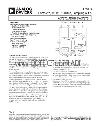
The AD7870, AD7875, and AD7876 are complete 12‑bit analog‑to‑digital converters from Analog Devices. They integrate a track‑hold amplifier, on‑chip reference, and multiple digital interfaces (parallel, byte, and serial) with low power consumption and fast data access times.
The document provides detailed electrical specifications, timing characteristics, package options, pin descriptions, and ordering guides for each part, along with reference circuit examples and performance graphs.
| Input Voltage Range (AD7870) | +3 V |
|---|---|
| Data Access Time | 57 ns |
| Signal‑to‑Noise Ratio (AD7870) | 72 dB at 10 kHz |
The AD7870 accepts a +3 V input range, the AD7875 accepts 0 V to +5 V, and the AD7876 accepts a +10 V input range.
The AD7870 is a low‑power device with typical consumption of about –60 mW.
The maximum data access time is 57 ns.