
The document describes the features and characteristics of the AD9878 mixed-signal front end for broadband applications.
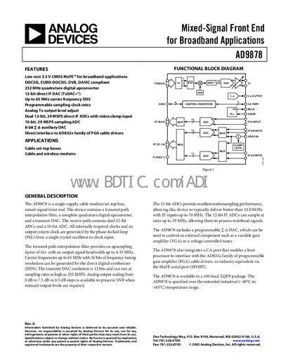
The AD9878 is a single‑supply, mixed‑signal front‑end designed for cable modems and set‑top boxes. It integrates a transmit‑path interpolation filter, a quadrature digital upconverter, a 12‑bit transmit DAC, dual 12‑bit IF ADCs, and a 10‑bit ADC, all powered from a 3.3 V supply. The device includes programmable clock rates, analog output level control, and a CA port for interfacing with AD832x PGA cable drivers.
The document provides electrical characteristics, absolute maximum ratings, pin configuration, register definitions, timing specifications, and ordering information. It also includes functional block diagrams, performance tables, and PCB design guidelines for implementing the AD9878 in broadband applications.
| Supply Voltage (VDD) | 3.3 V ±5 % (Vas) / ±10 % (Vos) |
|---|---|
| Maximum Sample Rate (Tx DAC) | 232 MHz |
| Tx DAC Resolution | 12 bits |
| 12‑bit ADC Maximum Conversion Rate | 29 MHz |
| 10‑bit ADC Maximum Conversion Rate | 29 MHz |
| Operating Temperature Range | -40 °C to +85 °C |
| Package | 100‑lead LQFP |
| Supply Current (Full Operation) | 184 mA (typical) |
The device is specified for an extended industrial temperature range of –40 °C to +85 °C.
The absolute maximum rating for the supply voltage is 3.9 V.
The transmit DAC can operate at up to 232 MHz sample rate.
The AD9878 is offered in a 100‑lead LQFP package.