
The AD743 is an ultralow noise, precision, FET input operational amplifier with excellent DC and AC performance.
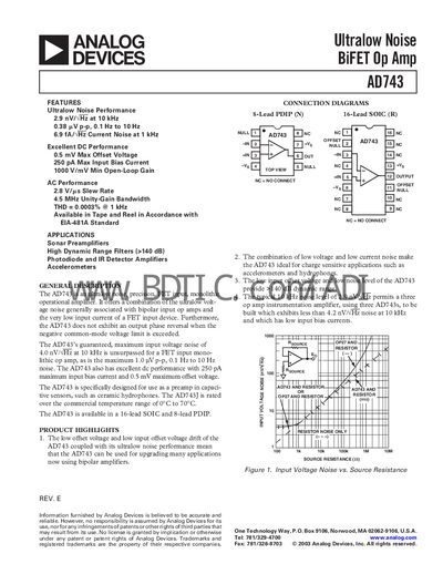
The AD743 is an ultralow‑noise JFET input operational amplifier offering 2.9 nV/√Hz voltage noise at 10 kHz, 0.38 V p‑p noise from 0.1 Hz to 10 Hz, and a 0.5 mV maximum offset voltage. It delivers 4.5 MHz unity‑gain bandwidth, 2.8 V/µs slew rate, and low input bias current (150 pA typical at 0 V).\n\nThe device is supplied in 8‑lead PDIP (N) and 16‑lead SOIC (R) packages and is intended for low‑noise applications such as sonar preamplifiers, high‑dynamic‑range filters, photodiode amplifiers, and accelerometer signal conditioning. The datasheet includes absolute maximum ratings, detailed electrical specifications, typical performance graphs, and recommended external circuitry for charge‑amplifier designs.
| Input Offset Voltage (Initial) – Min | 0.25 mV |
|---|---|
| Input Offset Voltage (Initial) – Typ | 1.0 mV |
| Input Bias Current (Either Input, V‑ = 0 V) – Min | 150 pA |
| Input Bias Current (Either Input, V‑ = 0 V) – Typ | 400 pA |
| Input Voltage Noise @ 10 kHz – Min | 2.9 nV/√Hz |
| Input Voltage Noise @ 10 kHz – Typ | 4.0 nV/√Hz |
| Unity‑Gain Bandwidth | 4.5 MHz |
| Operating Supply Voltage Range | +4.8 V to +18 V |
| Quiescent Current | 8.1 mA to 10.0 mA |
| Package Types | 8‑Lead PDIP (N) and 16‑Lead SOIC (R) |
The initial input offset voltage is specified as 0.25 mV minimum and 1.0 mV typical.
The AD743 exhibits a typical input voltage noise of 4.0 nV/√Hz at 10 kHz.
The device is offered in an 8‑lead PDIP (N) package and a 16‑lead SOIC (R) package.
It operates from +4.8 V up to +18 V.