
This document introduces the features and characteristics of AD8682/AD8684 dual/quad low power, high speed JFET operational amplifiers, including low supply current, high slew rate, bandwidth, low offset voltage, low input bias current, CMRR, fast settling time, unity gain stable.
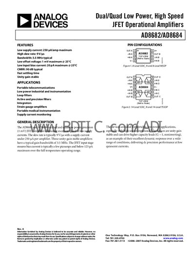
The AD8682 and AD8684 are dual/quad JFET input operational amplifiers designed for low‑power industrial, telecommunications and medical instrumentation. They feature ultra‑low supply current, low offset voltage, high slew rate and unity‑gain stability.
Key specifications include a typical supply current of 250 pA per amplifier, a slew rate of 9 V/µs, a gain‑bandwidth product of 3.5 MHz, CMRR of 90 dB typical, and an absolute maximum supply voltage of +18 V. The devices are available in 8‑lead SOIC, 8‑lead MSOP, 14‑lead TSSOP and 14‑lead SOIC packages.
| Supply Current per Amplifier | 250 pA typical |
|---|---|
| Gain‑Bandwidth Product | 3.5 MHz |
| Input Offset Voltage | 1 mV max @ 25 °C |
The typical supply current is 250 pA per amplifier at 25 °C.
The gain‑bandwidth product is 3.5 MHz.
The absolute maximum supply voltage is +18 V.