
The document describes the features and characteristics of the AD650 V/F/V (voltage-to-frequency or frequency-to-voltage converter), including high frequency conversion, reliable monolithic construction, low nonlinearity, and adjustable input offset to zero.
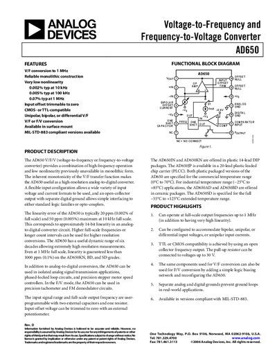
The AD650 provides high‑frequency V/F and F/V conversion with very low nonlinearity (0.002 % typ at 10 kHz). It supports unipolar, bipolar, and differential inputs, and features an open‑collector output compatible with CMOS or TTL logic. The device is suitable for precision analog‑to‑digital conversion, isolated signal transmission, PLL circuits, and tachometer applications.
The converter is offered in several packages, including 14‑lead plastic DIP, 20‑lead PLCC, and side‑brazed ceramic DIP, covering commercial (0 °C‑70 °C), industrial (‑25 °C‑85 °C), and extended‑temperature (‑55 °C‑125 °C) ranges. Detailed specifications, pin functions, and component‑selection guidelines are provided for designers.
| Full‑Scale Frequency Range | 1 MHz |
|---|---|
| Nonlinearity at 10 kHz | 0.002 % typ |
| Voltage Input Range | -10 V to 0 V |
| Open‑Collector Output Voltage Range | 0 V to 36 V |
| Absolute Maximum Total Supply Voltage | 36 V |
| Input Offset Voltage (Trimmable) | ±4 mV |
The AD650 can generate a full‑scale output frequency of up to 1 MHz.
Typical nonlinearity at 10 kHz is 0.002 %.
A pull‑up resistor that limits the output current to 8 mA is recommended; for a 5 V logic supply this means at least 625 Ω.