
This manual covers the Digilent JTAG-HS3 programming cable for Xilinx FPGAs and SoCs, detailing software support, target device compatibility, design notes…
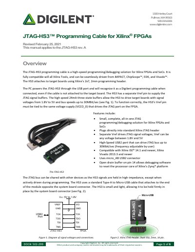
The JTAG-HS3 is a high-speed programming and debugging solution designed specifically for Xilinx FPGAs and SoCs. It connects directly to standard 2x7, 2mm Xilinx JTAG headers and supports signal voltages ranging from 1.8V to 5V with bus speeds up to 30 Mbit/sec. The cable features a separate Vref pin to supply JTAG signal buffers and is compatible with Xilinx tools such as iMPACT, ChipScope, EDK, and Vivado.
| Max Speed | 30 Mbit/sec |
|---|---|
| Voltage Range | 1.8V – 5V |
| Operating Temperature | -20 to +120 C (Storage) |
| Max DC Output Current | ±50 mA |
The JTAG-HS3 is compatible with Vivado 2014.1+, Vivado 2013.3+, and ISE 14.1+. It also supports ISE 13.1 – 13.4 with a specific Digilent Plugin.
Yes, it can drive this pin low to reset the processor core during debugging operations using an open drain buffer.
It cannot target Xilinx 9500/9500XL CPLDs, Xilinx 1700 and 18V00 ISP configuration PROMs, or support remote device configuration with iMPACT.