
Reference circuit guide for an HDMI‑to‑VGA converter using ADI parts, supporting up to 165 MHz HDMI and 1600×1200 @ 60 Hz video.
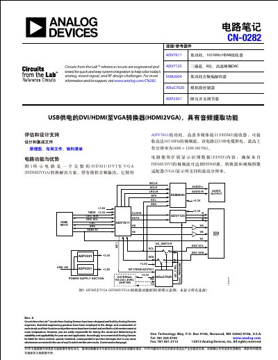
This document describes a complete HDMI‑to‑VGA conversion solution (CN‑0282) built with ADI components such as the ADV7611 HDMI receiver, ADV7125 video DAC, SSM2604 audio codec, ADuC7020 microcontroller and ADP2301 buck regulator. The circuit is powered via USB and can handle video up to 165 MHz and a maximum resolution of 1600×1200 @ 60 Hz, with audio extraction via the built‑in HDMI audio packet extractor.
The guide includes a functional block diagram, detailed component descriptions, EDID handling procedures, PCB layout recommendations for 2‑ and 4‑layer boards, and a test setup using common HDMI sources and VGA monitors. Design support files (schematics, BOM, layout) are provided via the Analog Devices website. This manual is written in Chinese.
| HDMI receiver bandwidth | 165 MHz |
|---|---|
| Maximum video resolution | 1600 × 1200 @ 60 Hz |
| Power supply | USB 5 V |
| Audio codec sample rates | 44.1 kHz or 48 kHz LPCM |
| Microcontroller interface | I²C for component control |
It supports up to 1600 × 1200 pixels at 60 Hz.
The ADV7611 extracts audio packets and passes them to the SSM2604 codec, which supports LPCM at 44.1 kHz or 48 kHz.
EDID data is read from the VGA monitor, modified, and programmed into the ADV7611 so that the HDMI source sees only supported video and audio modes.
Yes, the design has been proven to work on a 2‑layer board at 165 MHz pixel clock.