
This datasheet details the specifications, electrical characteristics, and application information for the Analog Devices ADA4625-1 high-voltage, low-noise…
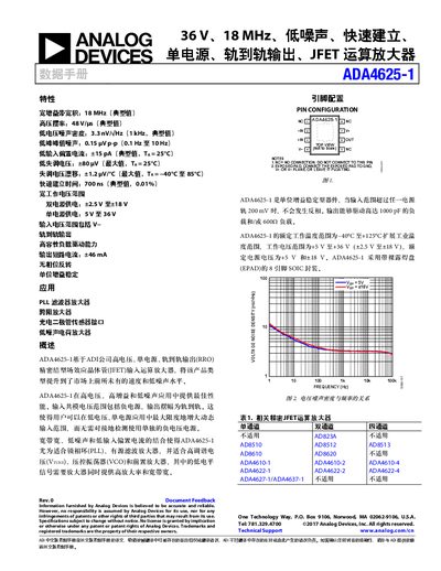
The document provides a comprehensive technical overview of the ADA4625-1, a precision JFET-input operational amplifier designed for high-voltage, single-supply, and rail-to-rail output applications. Key features include a wide gain-bandwidth product of 18 MHz, low voltage noise density, and fast slew rates suitable for PLL filters and transimpedance amplifiers.
The datasheet covers detailed electrical specifications under both ±18 V dual supply and 5 V single supply conditions, including input offset voltage, bias current, output swing, and dynamic performance metrics. It also includes absolute maximum ratings, thermal resistance data, pin configurations, and practical application circuit examples such as active loop filters for PLLs. This manual is written in Chinese.
| Gain Bandwidth Product (GBP) | 18 MHz (typical) |
|---|---|
| Slew Rate | 48 V/μs (typical) |
| Voltage Noise Density | 3.3 nV/√Hz at 1 kHz |
| Input Bias Current | ±15 pA (typical) |
| Output Short Circuit Current | ±46 mA |
| Operating Temperature Range | -40°C to +125°C |
| Supply Voltage Range (Dual) | ±2.5 V to ±18 V |
The device supports a dual supply range of ±2.5 V to ±18 V and a single supply range of 5 V to 36 V.
The typical input offset voltage (VOS) is ±80 μV when TA = 25°C.