
AAT3190 dual charge pump controller datasheet: 2.7V to 5.5V input, regulated positive and negative outputs up to ±25V, 30mA output current, 1MHz switching.
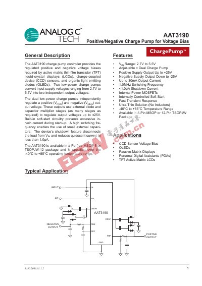
This datasheet describes the AAT3190, a positive/negative charge pump controller for voltage bias. It contains two low-power charge pumps that convert an input supply of 2.7V to 5.5V into two independent output voltages, regulating a positive output (VPOS) and a negative output (VNEG) using external diode and capacitor multiplier stages, up to ±25V. Built-in soft start limits in-rush current at start-up, and the shutdown feature disconnects the load from VIN and reduces quiescent current to less than 1.0µA.
The document covers pin descriptions and configuration for the 8-pin MSOP and 12-pin TSOPJW packages, absolute maximum ratings, electrical characteristics, typical performance curves, a functional block diagram, and a functional description of the negative and positive charge pump operating cycles. The AAT3190 is specified over the -40°C to +85°C temperature range and is aimed at TFT active-matrix LCDs, CCD sensor bias, OLEDs, passive-matrix displays and PDAs.
| Input Voltage Range | 2.7V to 5.5V |
|---|---|
| Output Voltage Range | up to ±25V |
| Output Current | Up to 30mA |
| Switching Frequency | 1.0MHz typical (0.8 to 1.2MHz) |
| Shutdown Current | less than 1.0µA |
| FBP Regulation Voltage | 1.2V nominal |
| Operating Temperature Range | -40°C to +85°C |
| Packages | Pb-free MSOP-8 or TSOPJW-12 |
It operates from an input supply ranging from 2.7V to 5.5V.
Using external diode and capacitor multiplier stages, the positive and negative outputs can be regulated up to ±25V.
The shutdown feature disconnects the load from VIN and reduces quiescent current to less than 1.0µA.
It is available in a Pb-free MSOP-8 or TSOPJW-12 package.