
ADSP-2191 is a DSP microprocessor developed by Analog Devices, with a 6.25ns instruction cycle time (internal), which can operate continuously at up to 160MIPS, is compatible with the ADSP-218x family code, and has single-cycle instruction execution, up to 16M words of addressable memory space, dual-purpose program memory for instruction and data storage, fully transparent instruction cache, unified memory space, independent ALU, multiplier/accumulator, bucket shifter calculation unit, two sets of calculation units and DAG registers Single-cycle environment switching, parallel execution of calculation and memory instructions, pipeline structure supports efficient code execution, register file calculation has all unconditional, no parallel calculation instructions, powerful program sequencer provides zero-cost loop and conditional instruction execution, and structure enhancement for compiled C code efficiency.
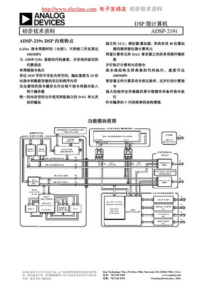
The ADSP-2191 is a single‑chip micro‑computing DSP optimized for high‑speed numeric processing. It features a 6.25 ns instruction cycle (160 MIPS), dual‑purpose program memory, a unified 24‑bit address space, and flexible power‑management with programmable PLLs.
The device includes 64 K words of on‑chip SRAM (32 K × 24‑bit program RAM + 32 K × 16‑bit data RAM), three SPORT serial ports, two SPI‑compatible ports, one UART, three programmable 32‑bit timers, up to 11 DMA channels, and is offered in 144‑pin LQFP or 114‑pin BGA packages.
| Instruction cycle time | 6.25 ns |
|---|---|
| Maximum processing speed | 160 MIPS |
| On‑chip SRAM | 64 K words (32 K × 24‑bit + 32 K × 16‑bit) |
| PLL multiplier range | 1× to 32× |
| Package options | 144‑pin LQFP (20×20×1.4 mm) or 114‑pin BGA (10×10×1.25 mm) |
The ADSP‑2191 operates with a 6.25 ns instruction cycle.
It provides 64 K words of SRAM, split into 32 K × 24‑bit program RAM and 32 K × 16‑bit data RAM.