
This document introduces Toshiba's RN49A2 transistor. The transistor is suitable for switching, inverter, interface, and driver circuits. It has 2 built-in elements and allows for device miniaturization and assembly simplification due to the built-in bias resistors.
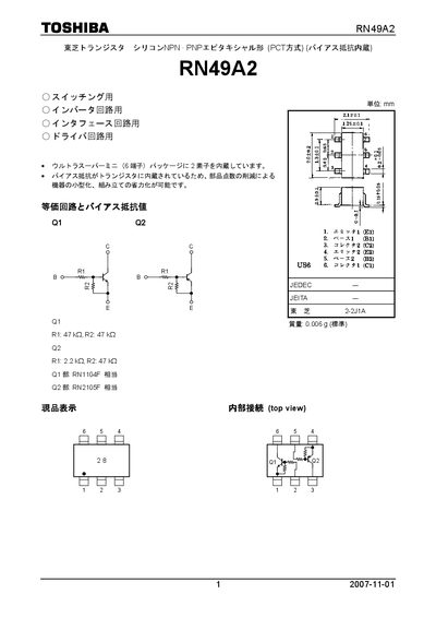
The RN49A2 is a silicon NPN/PNP epitaxial transistor with built‑in bias resistors, intended for switching, inverter, driver and other circuits. The document provides the absolute maximum ratings, detailed electrical parameters, and package information for both Q1 and Q2 sections of the device.
Additional sections cover recommended handling, storage temperature limits, and legal notices. The data is presented in Japanese with standard electrical symbols and units, suitable for designers needing precise specifications for circuit design and reliability analysis. This manual is written in Japanese.
| Collector‑Base Voltage (VcBo) Q1 | 50 V |
|---|---|
| Collector‑Emitter Voltage (VcEo) Q1 | 50 V |
| Collector‑Base Voltage (VcBo) Q2 | -50 V |
| Collector‑Emitter Voltage (VcEo) Q2 | -50 V |
| Storage Temperature Range | -55 °C to 150 °C |
The maximum collector‑base voltage for Q1 is 50 V.
The device can be stored from –55 °C up to 150 °C.
The datasheet states the part is not intended for safety‑critical or high‑risk applications such as nuclear, aerospace, medical, or automotive systems.