
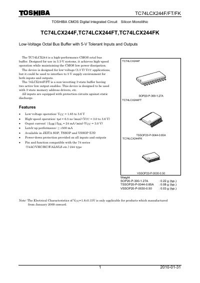
The TC74LCX244F/FT/FK from Toshiba is a high-performance CMOS octal bus buffer designed for use in 3.3-V systems. It is a non-inverting 3-state buffer with two active-low output enables, and the datasheet notes it can be used to interface to a 5-V supply environment for both inputs and outputs.
The document provides pin assignment, truth table, absolute maximum ratings, operating ranges, DC and AC electrical characteristics, test circuits and waveforms, and package dimensions for the SOP, TSSOP and VSSOP options.
| Operating temperature | -40 to 85 °C |
|---|---|
| Propagation delay time | 6.5 ns max (Vcc = 3.0 to 3.6 V) |
| Output current | 24 mA min (Vcc = 3.0 V) |
| Latch-up performance | > +500 mA |
| Package options | JEITA SOP, TSSOP and VSSOP (US) |
It operates from 1.65 to 3.6 V and is designed for use in 3.3-V systems.
The propagation delay time is 6.5 ns max when Vcc is 3.0 to 3.6 V.
It is a non-inverting 3-state buffer with two active-low output enables.
It is available in JEITA SOP, TSSOP and VSSOP (US) packages.