
The LTC2283 is a dual channel 12-bit 125Msps low power 3V ADC designed for digitizing high frequency, wide dynamic range signals. It is perfect for demanding imaging and communications applications with AC performance that includes 70.1dB SNR and 82dB SFDR.
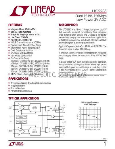
The LTC2283 is a 12‑bit, 125 Msps dual analog‑to‑digital converter designed for high‑frequency, wide‑dynamic‑range applications such as broadband communications and imaging. It operates from a single 3 V supply and offers low power consumption (≈790 mW) with flexible input ranges of 1 Vpp to 2 Vpp.
The datasheet provides detailed specifications, pin configurations, timing characteristics, and typical performance graphs. It also includes recommended solder‑pad dimensions for the 64‑lead QFN package and a list of related ADC parts for other sample rates and resolutions.
| Resolution | 12 bits |
|---|---|
| Maximum Sample Rate | 125 Msps |
| Supply Voltage | 2.85 V to 3.4 V |
| Power Dissipation (both channels, full speed) | 790 mW typical |
| Signal‑to‑Noise Ratio (5 MHz input) | 70.2 dB |
| Spurious‑Free Dynamic Range (5 MHz input) | 88 dB |
| Full‑Scale Bandwidth | 640 MHz |
| Input Range | 1 Vpp to 2 Vpp |
| Package | 64‑lead Plastic QFN (9 mm × 9 mm) |
The LTC2283 can sample at up to 125 Msps.
Typical power dissipation for both channels at full speed is 790 mW.
The device accepts differential input ranges from 1 Vpp to 2 Vpp.
The SNR is 70.2 dB at 5 MHz.