
This document introduces the basic features and hardware description of ZLG500 development board from Guangzhou Zhouligong Single-chip Microcomputer Development Co., Ltd., including development for mifare card reader module ZLG500A/B, 9V power supply, one-to-one and one-to-many communication, VC demonstration software and dynamic link library.
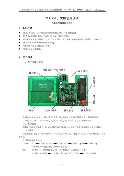
The ZLG500A/B development board is designed for developing applications with the MIFARE reader modules ZLG500A and ZLG500B. It operates from a 9 V supply, includes an internal 5 V regulator, and draws about 100 mA. The board offers both one‑to‑one RS232 and one‑to‑many RS485 master‑slave communication, with status indicators such as a buzzer and LED, and a reserved LCD interface.
Hardware description covers the RJ45 connector pinout, jumper groups JP1 and JP2 for selecting A‑type or B‑type module configurations, and the mapping of MCU pins to external drivers (MAX232, MAX485). Detailed jumper settings for each module type are provided, allowing users to configure the board for the desired communication mode. This manual is written in Chinese.
| Regulated voltage | 5 V |
|---|---|
| Typical current consumption | ≈100 mA |
| Communication interfaces | RS232 (point‑to‑point) and RS485 (master‑slave) |
| Status indicators | Buzzer and LED alarm |
By configuring the JP1 and JP2 jumpers on the board; different jumper settings enable A‑type or B‑type module operation.
It supports one‑to‑one RS232 communication and one‑to‑many RS485 master‑slave communication.