
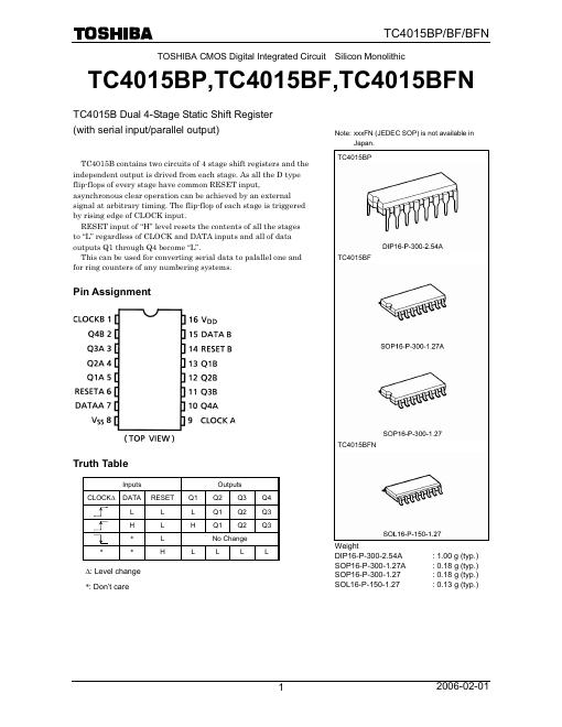
The TC4015BP/BF/BFN is a Toshiba CMOS digital integrated circuit containing two independent 4-stage shift registers with serial input and parallel output. All D-type flip-flops in each stage share a common RESET input, allowing asynchronous clearing by an external signal at arbitrary timing. Each flip-flop is triggered by the rising edge of the CLOCK input.
The device is available in DIP16, SOP16, and SOL16 packages, with typical weights of 1.00 g, 0.18 g, and 0.13 g respectively. Recommended DC supply voltage ranges from 3 to 18 V, and the operating temperature range is −40 to 85 °C.
| DC supply voltage | 3 to 18 V |
|---|---|
| Operating temperature range | −40 to 85 °C |
| Storage temperature range | −65 to 150 °C |
| DC input current | ±10 mA |
| Power dissipation | 300 mW (DIP) / 180 mW (SOIC) |
It is a CMOS dual 4-stage static shift register with serial input and parallel output.
It is achieved by an external RESET signal at arbitrary timing, resetting all stages to “L”.
The rising edge of the CLOCK input triggers each flip-flop stage.
No, the xxxFN (JEDEC SOP) package is not available in Japan.