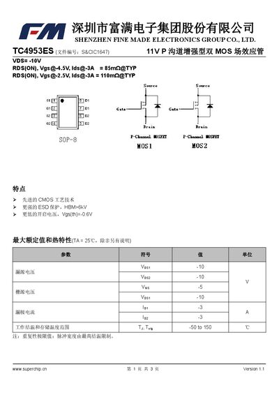
The TC4953ES is an 11 V P‑channel enhancement MOSFET with low on‑resistance and high ESD protection.
About this manual
The TC4953ES is a P‑channel enhancement MOSFET fabricated with advanced CMOS technology. It offers strong ESD protection (HBM > 6 kV) and a low gate‑threshold voltage of –0.6 V.
Key electrical ratings include a maximum drain‑source voltage of –10 V, a maximum gate‑source voltage of –5 V, and a continuous drain current of –3 A. Typical on‑resistance is 85 mΩ at VGS = –4.5 V and 110 mΩ at VGS = –2.5 V. The device is supplied in an SOP‑8 package. This manual is written in Chinese.
What's inside
- Features
- Maximum Ratings and Thermal Characteristics
- Electrical Characteristics
- Package Information
Specifications
| Maximum Drain‑Source Voltage (VDS) | -10 V |
|---|
| Maximum Gate‑Source Voltage (VGS) | -5 V |
|---|
| Continuous Drain Current (ID) | -3 A |
|---|
| ESD Protection (HBM) | > 6 kV |
|---|
| Package | SOP‑8 |
|---|
Frequently asked questions
What is the maximum drain‑source voltage of the TC4953ES?
The maximum drain‑source voltage is –10 V.
What ESD protection level does the device provide?
It provides ESD protection greater than 6 kV (HBM).
In which package is the TC4953ES supplied?
The device is supplied in an SOP‑8 package.