
74AUP1G04 is a low voltage CMOS single inverter gate fabricated with sub-micron silicon gate and double-layer metal wiring C2MOS technology. It is ideal for 1.2 to 3.6 V operations and low power and low noise applications. All inputs and outputs are equipped with protection circuits against static discharge, giving them 2kV ESD immunity and transient excess voltage.
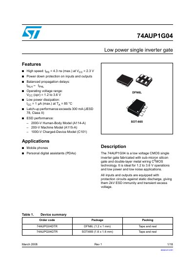
This document is a datasheet for the 74AUP1G04, a low voltage CMOS single inverter gate designed for mobile phones and personal digital assistants. It operates within a voltage range of 1.2 to 3.6 V and features high speed with a maximum propagation delay of 4.3 ns. The device includes power down protection on inputs and outputs and is available in DFN6L and SOT-665 packages.
The datasheet provides comprehensive technical specifications, including absolute maximum ratings, recommended operating conditions, and DC and AC electrical characteristics. It also details pin assignments, truth tables, and test circuit configurations for the device.
| Operating voltage range | 1.2 to 3.6 V |
|---|---|
| Maximum propagation delay | 4.3 ns |
| Power dissipation | 1 µA (max.) |
| Latch-up performance | 300 mA |
| ESD performance (Human-Body Model) | 2000 V |
| ESD performance (Machine Model) | 200 V |
| ESD performance (Charged-Device Model) | 1000 V |
| Supply voltage (Absolute Max) | -0.5 to +4.6 V |
| Operating temperature | -40 to 85 °C |
| Input capacitance | 8 pF |
The device is ideal for mobile phones and personal digital assistants (PDAs).
The maximum propagation delay is 4.3 ns at a supply voltage of 2.3 V.
The recommended operating voltage range is 1.2 to 3.6 V.
The device is available in DFN6L and SOT-665 packages.