
The document describes the features and characteristics of the 74LCX245 low voltage CMOS octal bus transceiver. It has 5V tolerant inputs and outputs, and is suitable for low power and high speed 3.3V applications. This product is intended for two-way asynchronous communication between data buses, with the direction of data transmission determined by the DIR input. The enable input G can be used to disable the device, effectively isolating the buses. All inputs and outputs are equipped with protection circuits against static discharge, providing 2KV ESD immunity and transient excess voltage protection. All floating bus terminals during the High Z state must be held HIGH or LOW.
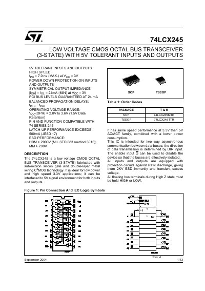
The STMicroelectronics 74LCX245 is a low voltage CMOS octal bus transceiver with 3-state outputs, fabricated with sub-micron silicon gate and double-layer metal wiring C2MOS technology. It is intended for two-way asynchronous communication between data buses, with data direction set by the DIR input and bus isolation through the G enable input.
The datasheet covers pin connections and functions, truth table, absolute maximum ratings, recommended operating conditions, DC and AC specifications, test circuits, package mechanical data, and revision history. It lists SOP and TSSOP order codes.
| Operating Supply Voltage | 2.0 V to 3.6 V |
|---|---|
| Input Voltage Range | 0 to 5.5 V |
| High or Low Level Output Current | ±24 mA at VCC = 3 V |
| Propagation Delay | 7.0 ns max at VCC = 3 V |
| Operating Temperature | -55 to 125 °C |
The recommended operating supply voltage range is 2.0 V to 3.6 V, with 1.5 V data retention.
The direction of data transmission is determined by the DIR input.
The G enable input can disable the device so the buses are effectively isolated.
The maximum propagation delay is 7.0 ns at VCC = 3 V.