
The VND1NV04, VNN1NV04, VNS1NV04 are monolithic devices designed in STMicroelectronics® VIPower® M0-3 Technology, intended for replacement of standard Power MOSFETs from DC up to 50 KHz applications. Built in thermal shutdown, linear current limitation and overvoltage clamp protect the chip in harsh environments. Fault feedback can be detected by monitoring the voltage at the input pin.
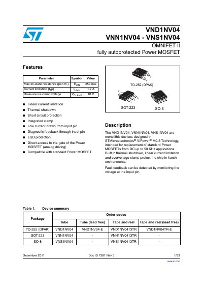
The VND1NV04, VNN1NV04, and VNS1NV04 are monolithic devices designed in STMicroelectronics VIPower MO-3 Technology. They function as fully autoprotected Power MOSFETs intended for replacement of standard Power MOSFETs in DC up to 50 KHz applications.
| Max on-state resistance (per channel) | 250 mΩ |
|---|---|
| Current limitation (typical) | 1.7 A |
| Drain-source clamp voltage | 40 V |
| Operating junction temperature | Internally limited |
| Storage temperature range | -55 to 150 °C |
The maximum on-state resistance per channel is 250 mΩ.
The maximum on-state resistance is 250 mΩ.
The typical linear current limitation is 1.7 A.
The maximum drain-source clamp voltage is 40 V.