
This is an application note about boost circuit optimization parameters, which introduces the optimization parameters of boost circuit, including the value of input capacitor Ci, the current ripple in the boost inductor Lb, the parasitic capacitances of the boost inductor and power semiconductors, the operating frequency and also the frequency modulation technique.
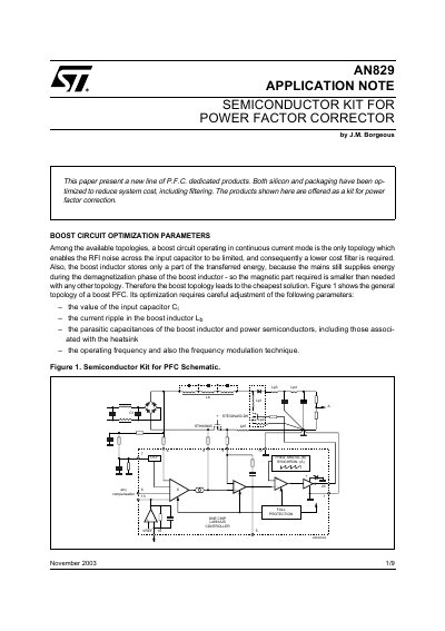
This document presents a new line of dedicated products for power factor correction (PFC), optimized to reduce system cost including filtering. The proposed solution utilizes a boost circuit operating in continuous current mode to limit RFI noise and minimize magnetic component size. The semiconductor kit consists of an L4981 controller, an STE36N50-DK power module, and an STH80N05 power sense component.
The L4981 controller operates with an input voltage range of 85V to 270V using average current mode PWM control. It features feed-forward line and load compensation, overvoltage and overcurrent protection, and soft start. The STE36N50-DK power module integrates a low Rds(on) Power MOSFET and a TURBOSWITCH Diode in an isolated ISOTOP package. The STH80N05 power sense uses a high-density low-voltage Power MOSFET for current sensing, offering low resistance and intrinsic diode protection.
| Input voltage range | 85V to 270V |
|---|---|
| Output voltage | 400Vdc |
| Switching frequency | below 50kHz |
| MOSFET Rds(on) | 0.14 Ohm |
| Diode reverse voltage | 600V |
| Diode forward voltage | 1.5V |
The kit consists of an L4981 controller, an STE36N50-DK power module, and an STH80N05 power sense.
The switching frequency is kept below 50kHz to maintain RFI noise within the optimum frequency range of the VFG 243 standard.
A material with distributed air gaps, such as iron powder, is recommended as a good choice.