
This application note describes how to connect the TDA7498 demonstration board, how to evaluate the performance of the demonstration board using the electrical curves, and how to avoid critical issues in the PCB schematic and layout of the TDA7498E.
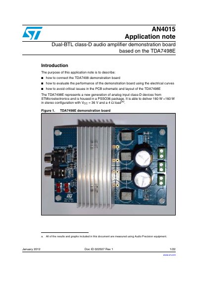
The document provides instructions on how to connect the TDA7498E demonstration board and evaluate its performance using electrical curves such as THD+N versus power and frequency. It details the test conditions, including power supply connections and output configuration in 2-channel BTL mode.
Additionally, the note offers design guidelines for PCB schematic and layout, covering component selection, decoupling capacitors, output filters, and specific routing strategies for signal and ground planes to avoid critical issues.
The device is able to deliver 160 W +160 W in stereo configuration with Voc = 36 V and a 4 Ω load.
The device is housed in a PSSO36 package.