
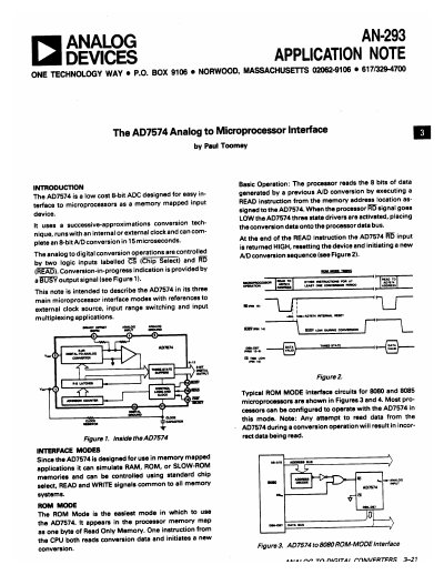
The document provides an overview of the AD7574, a low-cost 8-bit analog-to-digital converter (ADC) designed for easy interfacing with microprocessors. It utilizes a successive-approximations conversion technique capable of completing an 8-bit A/D conversion in 15 microseconds. The device is controlled via logic inputs labeled CS (Chip Select) and RD (READ), with conversion status indicated by a BUSY output signal.
The note details three primary interface modes for the AD7574: ROM Mode, RAM Mode, and Slow Memory Mode. It explains the basic operation of each mode, including how they simulate memory types like RAM or ROM within a processor's memory map. The document also covers timing considerations, such as the requirement for CS to return HIGH within 250ns after RD goes HIGH in RAM mode, and discusses applications involving range switching using the AD7574's input pins.
The device can complete an 8-bit A/D conversion in 15 microseconds.
The maximum value for the internal reset cycle is 250ns at 25°C.
The mode is intended for use with processors that can be forced into a wait state for at least 15ps.