
The NC7WZ241 is a Dual Non-Inverting Buffer with 3-STATE outputs. The device is fabricated with advanced CMOS technology to achieve superior switching performance and high output drive while maintaining low static power dissipation. It is specified to operate over the 1.65V to 5.5V VCC operating range. The inputs and outputs are high impedance when VCC is 0V. Outputs can tolerate voltages above VCC when in the 3-STATE condition.
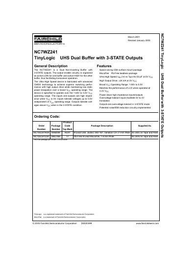
The NC7WZ241 is a dual non-inverting buffer with 3-STATE outputs manufactured by Fairchild Semiconductor using advanced CMOS technology. The device features active LOW enable for one buffer and active HIGH enable for the other, facilitating transceiver operation. It is specified to operate over a broad supply voltage range of 1.65V to 5.5V.
| Supply Voltage Operating Range | 1.65V to 5.5V |
|---|---|
| Propagation Delay (Typical) | 2.6 ns |
| Output Drive Current | ±24 mA |
| Operating Temperature Range | -40°C to +85°C |
| Storage Temperature Range | -65°C to +150°C |
| Package Types | US8 and MicroPak |
The device is specified to operate over the 1.65V to 5.5V VCC operating range.
The output enable circuitry is organized as active LOW for one buffer and active HIGH for the other buffer.
The inputs and outputs are high impedance when VCC is 0V.