
The NC7WP240 is a Dual Inverting Buffer with independent active LOW enables for the 3-STATE outputs. It is ideal for applications where battery life is critical. This product operates within the VCC range of 0.9V to 3.6V and has ultra low power consumption. It is designed with advanced CMOS technology to achieve high speed performance and extremely low power dissipation.
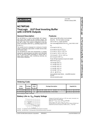
The NC7WP240 is a Dual Inverting Buffer featuring independent active LOW enables for its 3-STATE outputs. It is an Ultra High Power (ULP) device ideal for battery-powered applications where extending battery life is critical due to extremely low static and dynamic power consumption.
The internal circuit utilizes a minimum number of inverter stages, including the output buffer, to achieve best-in-class speed operation while maintaining ultra-low CMOS power dissipation. The device operates with an optimized supply voltage range from 0.9V to 3.6V.
| Supply Voltage Range | 0.9V to 3.6V |
|---|---|
| Operating Temperature Range | -40°C to +85°C |
| Static Drive Current @ 3.0V | 42.6 mA |
| Propagation Delay (Typ) @ 3.6V | 3.0 ns |
The device operates with a supply voltage (Vcc) ranging from 0.9V to 3.6V.
The NC7WP240 operates with a supply voltage between 0.9V and 3.6V.
The device can be stored in temperatures from -65°C to +150°C.