
This document is downloaded from www.AllDataSheet.com and contains datasheets from various manufacturing companies. These datasheets are 100% free and can be downloaded without registration. The document provides a fast search system for users to easily find the desired datasheets. It is important to note that all datasheets cannot be modified without permission.
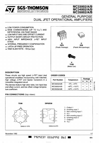
These circuits are high speed J-FET input dual operational amplifiers incorporating well matched, high voltage J-FET and bipolar transistors in a monolithic integrated circuit. The devices feature high slew rates, low input bias and offset current, and low offset voltage temperature coefficient.
| Supply Voltage Range (MC34002) | -55 to +125 °C |
|---|---|
| Supply Voltage Range (MC35002) | -65 to +150 °C |
| Slew Rate | 16 V/us (typ) |
Yes, the device includes internal frequency compensation.
The absolute maximum rating for the supply voltage (Vcc) is 18 V.
The MC34002/A/B models operate from 0 to 70 °C, while the MC35002/A/B models operate from -55 to 125 °C.
The high slew rate is typically 16 V/us.