
This document is a product description for CD4071BM-CD4071BC Quad 2-Input OR Buffered B Series Gate CD4081BM-CD4081BC Quad 2-Input AND Buffered B Series Gate
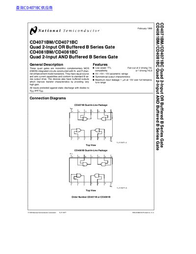
This document is a technical datasheet for the CD4071BM and CD4071BC, which are monolithic complementary MOS (CMOS) integrated circuits. These devices feature four 2-input OR gates with buffered outputs designed to improve transfer characteristics by providing very high gain.
| Supply Voltage Range | 5V to 15V |
|---|---|
| Operating Temperature Range (BM) | -55°C to +125°C |
| Operating Temperature Range (BC) | -40°C to +85°C |
| Maximum Power Dissipation (Dual-In-Line) | 700 mW |
| Maximum Power Dissipation (Small Outline) | 500 mW |
| Storage Temperature Range | -65°C to +150°C |
The maximum input leakage is 1 pA at 15V over the full temperature range.
The maximum power dissipation for a Dual-In-Line package is 700 mW.
The operating voltage range is from 3 V to 15 V.