
The ADN2813 is a Clock and Data Recovery IC with Integrated Limiting Amplifier that supports a continuous rate of 10 Mb/s to 1.25 Gb/s. It exceeds SONET requirements for jitter transfer/generation/tolerance and features adjustable slice level, independent slice level adjust and LOS detector, no reference clock required, etc.
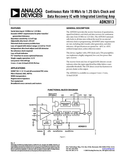
The ADN2813 is an Integrated Circuit designed to provide receiver functions including quantization, signal level detection, and clock and data recovery. It supports serial data input rates from 10 Mb/s up to 1.25 Gb/s and meets SONET requirements for jitter transfer, generation, and tolerance without requiring a reference clock.
The device is available in a compact 32-lead LFCSP package with single-supply operation at 3.3 V. Key features include an adjustable slice level, independent loss-of-signal (LOS) detection, and low power consumption of approximately 450 mW typical.
| Data Rate Range | 10 Mb/s to 1.25 Gb/s |
|---|---|
| Supply Voltage | 3.3 V |
| Operating Temperature Range | -40°C to +85°C |
| Package Type | 32-lead LFCSP |
No, it does not require an external reference clock or programming to automatically lock to all data rates.
The device has a low power consumption with a typical value of 450 mW.
The LOS detect range is between 2.3 mV and 19 mV.