
The LTC1749 is an 80Msps, 12-bit A/D converter designed for digitizing wide dynamic range signals up to frequencies of 500MHz. The input range of the ADC can be optimized with the on-chip PGA sample-and-hold circuit and flexible reference circuitry.
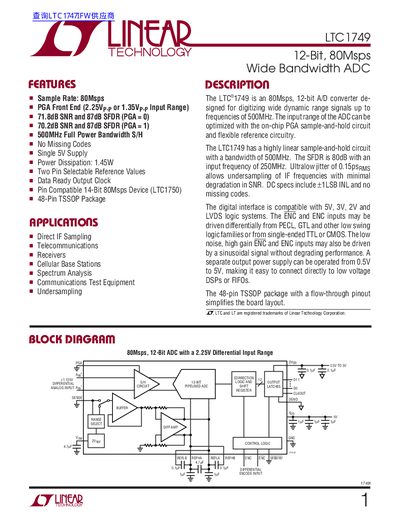
The LTC1749 is a 12‑bit, 80 Msps analog‑to‑digital converter designed for high‑speed, wide‑bandwidth applications such as direct‑IF sampling, telecommunications receivers, and spectrum analysis. It features a selectable on‑chip PGA, low jitter (0.15 ps), and a 48‑lead TSSOP package that simplifies board layout.
The device offers a full‑scale input range of up to 5 V, low power dissipation (≈1.45 W), and a digital interface compatible with 5 V, 3 V, 2 V, and LVDS logic families. Detailed electrical characteristics, timing parameters, and typical performance graphs are provided throughout the document.
| Sample Rate | 80 Msps |
|---|---|
| Resolution | 12 bits |
| Power Dissipation | 1.45 W (typical) |
| Supply Voltage (Vop) | 4.75 V – 5.25 V |
| Package | 48‑lead plastic TSSOP |
The LTC1749 can sample at up to 80 Msps.
Typical power dissipation is 1.45 W.
It is supplied in a 48‑lead plastic TSSOP package.
The converter provides a 12‑bit resolution with no missing codes.