
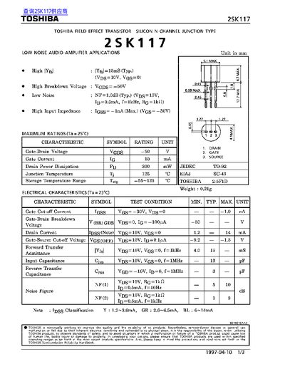
This document describes the Toshiba 2SK117 silicon N‑channel junction field‑effect transistor. It includes maximum ratings such as voltage, current, power dissipation, and temperature limits, as well as detailed electrical characteristics measured under specified test conditions.
Key sections cover static and dynamic characteristics, common‑source configurations, forward transfer admittance, and noise performance. The data are intended for designers to evaluate the device in low‑noise audio amplifier applications and other circuits.
| Gate‑Drain Voltage (Vgd) | -50 V (max) |
|---|---|
| Gate Current (Ig) | 10 mA (max) |
| Drain Power Dissipation (Pp) | 300 mW (max) |
| Junction Temperature (Tj) | 125 °C (max) |
| Storage Temperature Range (Tstg) | -55 °C to 125 °C |
| Noise Figure (NF) | 1.0 dB (typ) |
The maximum gate‑drain breakdown voltage is -50 V.
The typical noise figure is 1.0 dB.
The device can be stored from -55 °C up to 125 °C.